We stock a large number of various high precision/low-power analog IPs. If you need, based on existing design data, we can convert analog IP process. We have developed powerful tool called FPNA (Floor Plan Noise Analysis) to achieve robust floor plan early in the design.
High-Performance Analog IP
》Analog IP List & Datasheet (user name, password is required)
If you would like to browse, please send e-mail to the address below. We disclose password immediately to you.
e-mail: info@a-r-tec.jp
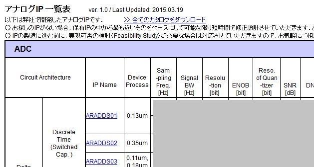
Image of Analog IP List:
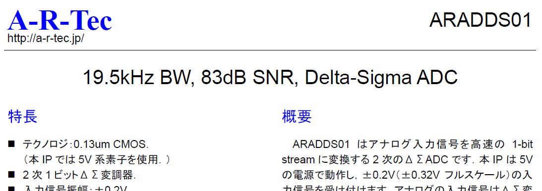
 Image of Analog IP Datasheet:

ADC

- ΔΣADC -- high-resolution, high-precision, high-SNR ex. 1 BW: 20kHz, fs: 10MHz, SNR: 80dB, Power: 15mW, App: control, FA ex. 2 BW: 20kHz, fs: 2MHz, SNR: 95dB, Power: 0.6mW, App: portable device ex. 3 BW: 100MHz, fs: ∼5GHz, SNR: 70dB, App: wireless communications (broadband)
- Successive approximation ADC --low-power, high-precision ex. 1 resolution: 14-bit, fs: 128kHz, DNL: ±0.5LSB, Current: 1mA ex. 2 resolution: 12-bit, fs: 2MHz, DNL: ±0.5LSB, Current: 0.5mA
- Flash ADC -- high-speed, low-resolution ex. 1 resolution: 4-bit, fs: 300MHz, Background calibration, App: ΔΣADC ex. 2 SiGe-HBT, BW: 2GHz, resolution: 3-bit, App: high-frequency measurement
- Pipelined ADC -- high-precision, high-speed
- Counter ADC -- for image sensor
ADC performance region and A-R-Tec's experience:
DAC

- ΔΣDAC ex. 1 BW: 100kHz, Input: 16-bit, fs: ∼20MHz, SNR: 90dB, MASH ex. 2 BW: 10kHz, fs: 5MHz, SNR: 120dB, Noise Floor: 60nV/rtHz (ultra-low noise)
- Current summation DAC ex. 1 BW: 100kHz, Input: 8-bit, fs: 1MHz, ENOB: 7.6-bit, DNL: ±0.5LSB ex. 2 BW: Input: 4-bit, fs: 300MHz, DNL: ±0.5LSB, Background calibration, App: ΔΣADC
- Segmented R2R:R Ladder DAC ex. fs:∼1MHz, BW: ∼300kHz, Input: 16-bit, ENOB: 15-bit, DNL: ±1LSB
- R-string DAC ex. Input: 8-bit, DNL: ±1LSB, App: on-chip bias
- R2R DAC ex. Input: 10-bit, DNL: ±1LSB, App: on-chip bias
Low Noise Amp: LNA

- Capacitive feedback amp -- low-frequency (bio-signal, 0.01-1kHz), ultra-high resistance (∼100GΩ) ex. BW: 0.3-600Hz, Gain: 46-66dB, Input referred noise: 0.7uVrms (low noise)
- Chopper amp -- low-noise
Sensor Circuit

- Charge amp (CV converter) -- low-frequency (<100kHz), low-noise
MEMS pressure sensor, microphone, accelerometer/gyroscope sensor ex. Gain: 3V/pF, BW: ∼10kHz, ΔCin: ±0.3pF, Input referred noise: ∼10zF/rtHz - CMOS active pixel sensor -- low-noise, high-DR
visible light, x-ray
SOI CMOS, Bulk CMOS - Substrate noise sensor (for on-chip noise detection)
- Temperature sensor (for temperature measurement of the chip)
VCO

- Ring oscillators -- low-frequency (<100MHz), small area
- LC-VCO -- high-frequency (1-10GHz), low phase noise, low-jitter
I/O Interface Circuit
- I/O circuit with ESD protection for mixed signal LSI
low leakage current, low-capacitance - I/O circuit with ESD protection for high voltage
We provide a brochure. If you would like to see, please send e-mail to the address below.
e-mail: info@a-r-tec.jp
Substrate Noise Analysis Tools (FPNA)
In analog-digital mixed LSI design, how to tame the transient supply current change during CMOS logic operation and its propagation in substrate, which cause cross-talk noise, has been one of the major issues. We have developed powerful tool called FPNA (Floor Plan Noise Analysis) to achieve robust floor plan early in the design.
Features:
- You can estimate the influence of cross-talk noise at the floorplan level before the detailed layout design.
- GDS data is no longer necessary. Based on the Si substrate resistivity and guard ring information, you can simulate in a short time.
- By applying FPNA for multiple floorplan ideas, you can find the best solution in a short time.
Analysis example:
》Nikkei technology online article
You can reduce the number of reworking and costs by the quantitative estimation of crosstalk noise by using FPNA. As a result, mixed signal LSI design is optimized, and design efficiency is increased. It is one of the essential key technologies in the development of mixed-signal LSIs having both analog/RF circuits of large dynamic range and large-scale logic circuits on a single die. Noise analysis technologies can be offered in various forms shown below.
》Brochure of FPNA ver. 1.0 (Japanese) 》Price of FPNA ver. 1.0 (Japanese) 》Comparison of the FPNA and GDS-based analysis (Japaese) 》FPNA ver. 1.0 Demo @EDS Fair 2010 (Japanese) 》Analysis example of FPNA ver. 1.0 (English) 》Related report (English)
We can also GDS-based simulation, please contact us.


