Noise Model and Analysis Flow
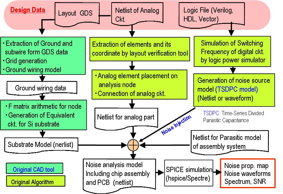
Model composition, Analysi procedure
- Input data is below.layout: GDSIIschematic: SPICE netlist (Analog), Verilog (digital)
- Extract ground lines from GDSII, place them on the resistive meshed Si. Calculate F-matrix and reduce the number of nodes by 2 orders of magnitude
- With TSDPC, model the noise calculated from logic simulation
- Integrate the substrate mode, analog and logic circuits, as well as bond wire/package elements
- Complte system level model
- AC, TRAN analysis with simulator
- Calculate the noise waveform, noise propagation/attenuation maps and noise spectrumlate
Chip Level Noise Analysis Model
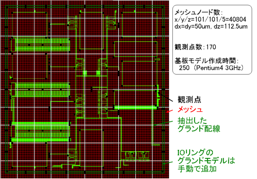
Modeling (1)
- Red: initial mesh
- Green: extranted GND lines: extracted ground
Simulate noise voltage with specified nodes for probing. Probing node should not be reduced. This example shows reduction of nodes from 40804 to 170.
Board-level Noise Analysis Model
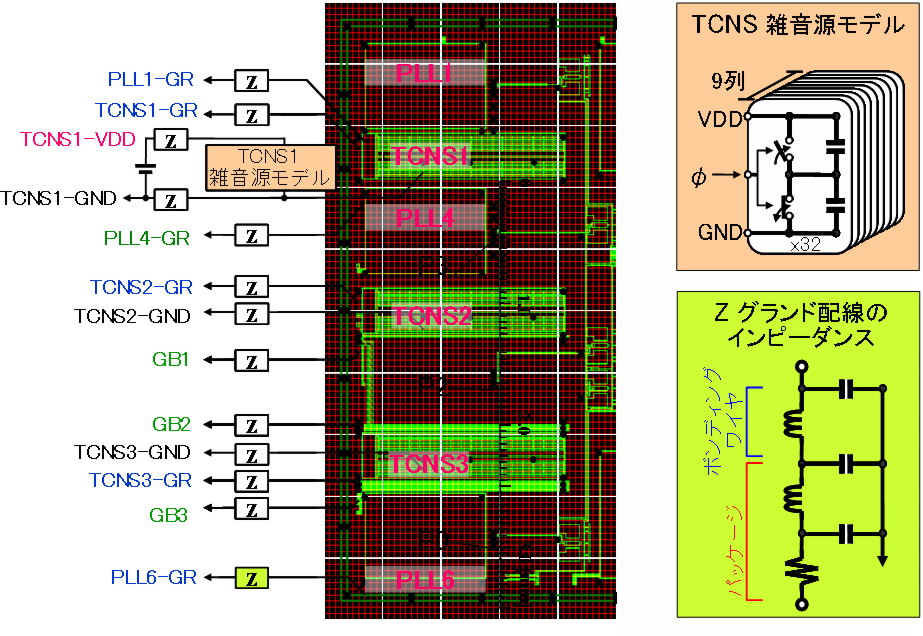
Modeling (2)
Consider the charging and discharging of the parasitic capacitance of CMOS logic circuits. Parasitic capacitance change with motion vectors.Wiring impedance considered, package leads, on the PCB pattern, on-chip metal wiring. Inductance becomes dominant in the high frequency region.
Simulation Result: Noise Propagation Map
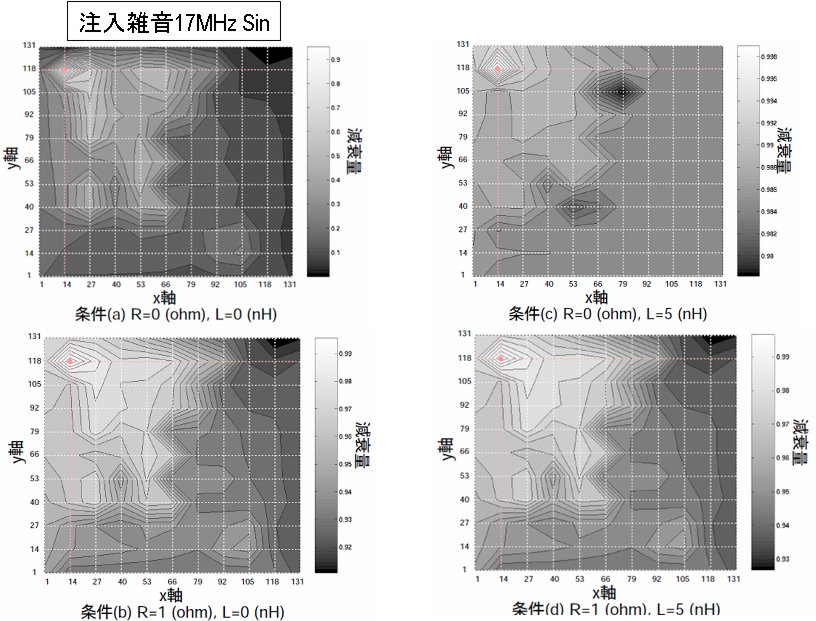
Chip surface distribution of propagated noise
- Shading shows the level of noise propagation at meshed analysis points.
- Noise source is given as DC/AC source at any analysis point.
- The areas connected to ground with low impedance shows less propagated noise.
Cross-Talk Noise Waveform
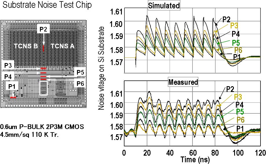
- Left: substrate noise test chip
- Upper right: simulation
- Bottom right: measurement
Good agreement in waveform structure and amplitude is obtained. Because of the wider bandwidth of noise transmission path and noise detector in simulation, the simulated waveform shows large high-frequency components.